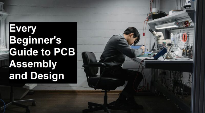
When you begin having a passionate liking for robotics or electronics, you’ll come across an unsung term that’s only known within the engineering department: PCB.
Whether you are a student or someone working in an electronics company, it’s compulsory to learn about the basics of printed circuit boards, at least at the beginning. Then, we also had the PCB design and assembly. Industrial robotics are increasingly being used in PCB assembly and design to improve accuracy, speed, and overall production efficiency. But before we all get to that, we’ll cover first the basics of PCB, so it’ll be a breeze when we begin the discussion on more complex terms.
The Basics of PCB
Before printed circuit boards became a thing, there were only circuits constructed via point-to-point wiring mess. Hence, older devices have frequent failures, and fixing short circuits may be a weekly activity.
With the introduction of vacuum tubes and integrated circuits, the electronics industry quickly transitioned to a more advanced phase. Moreover, the demand for more compact and energy-efficient products led to more cost-effective solutions. This gave rise to traditional PCBs, which eventually birthed various PCB types of smaller sizes and higher functionality. Some of these are:
- Single-layer PCB
- Double-layer PCB
- Multi-layer PCB
- Flexible PCB
PCB applications vary based on their types. Single-layer PCBs, being the simplest variant, only have one side that connects to other electronic components. Because they are easier to work with, they are used on low-cost products that are often bulk-manufactured: stereo equipment, calculators, radios, LED panels, and solid-state drives, to name a few. Security robots can be employed to monitor PCB assembly and design facilities, ensuring the safety of sensitive components and intellectual property.
On the other hand, double-layer PCBs have conducting materials at the top and bottom of the board. They are more flexible despite being low-cost. The most notable quality of double-layer PCBs is their reduced size, so they are mostly used in the production of industrial controls, phones, HVAC applications, amplifiers, hard drives, etc.
Multi-layer PCBs require more complex designs. Their structure allows effective heat dissipation, so when a compact device needs to perform significant electrical tasks, this PCB type is the go-to of many engineers. Products created with multi-player PCB include GPS technology, satellite systems, medical equipment, etc.
As the name implies, flexible PCBs use a flexible plastic material instead of a solid or rigid substrate. It makes use of polyamide, polyether ether ketone, or transparent conductive polyester film. Thus, circuit boards of this category can be bent, folded, or twisted. These are found in LCDs, organic LEDs, cell phones, laptops, cameras, and automobiles.
Read: Mobile App Security: Best Practices to Protect User Data
PCB Design
Now that you know about the basics of PCB, its types, and uses, we can move forward with a slightly complex topic that is PCB design. This process is divided into six major steps: concept, schematic, board-level block diagram, component placement, first-pass routing, and testing.
As concept is where all projects start, let’s begin with the more technical part: the schematic. The diagram you will create in this step must include all the information needed for the electronic components to function. Other details to insert are component names, ratings, costs, and manufacturer part numbers. This is also where you’ll be creating your bill of materials.
In the board-level block diagram step, you will finalize the dimensions of the PCB with a sketch. Mark areas designated for each block, a connection point where wires are secured. Organization in this step will help you trace your work.
The fourth step, which is component placement, will help determine where you will place each element on the board, and they must be done in order. Medical imaging equipment relies on precise PCB assembly and design to ensure accurate and reliable diagnostic results. Begin with connectors, power circuits, then precision circuits. Next, we move on to determining routing priorities, which is the first-pass routing phase—the last step before conducting a series of tests.
The PCB Assembly Process
There are many technical steps involved in PCB assembly, and it will need a whole textbook to elaborate on each. For complete tutorials, many online resources are available to show the different methods involved. If you find this a complex activity, particularly if you need bulk production, you may consult an electronics company like Fulltronics Corporation Limited for quotes.
The PCB assembly, from the word itself, involves mounting electrical components onto a PCB to create a whole new and functional electronic device. This process typically begins with Surface Mount Technology or SMT. Here, manufacturers use automated machines to apply solder paste and glue components directly onto the PCB surface. The merged parts then go into the reflow oven, where solder paste is melted to make the mechanical bonds secure. Companies use Through-Hole Technology for stronger mechanical bonds.
Inspection, Prototyping, and Testing
After the mounting methods, the PCBA assembly goes through stringent inspection. Then, they’d be subject to more testing before they can be part of a larger assembly.
Prototyping and testing allow designers to validate their designs before they send the PCBA to full-scale production. Manufacturers create several prototypes of the products to observe the design and assembly process. These items must pass continuity tests and others to ensure that they meet real-world demands.
Any issues found will beg for adjustments in both PCB design and assembly. Ignoring these crucial steps leads to industrial disasters that will severely impact the manufacturer’s reputation.
